Thursday, July 8, 2010
Astable Multivibrator
The output remains at each voltage level for a definite period of time. If you looked at this output on an oscilloscope, you would see continuous square or rectangular waveforms. The astable multivibrator has two outputs, but NO inputs.
Let's look at the multivibrator in figure 3-3 again. This is an astable multivibrator. The astable multivibrator is said to oscillate. To understand why the astable multivibrator oscillates, assume that transistor Q1 saturates and transistor Q2 cuts off when the circuit is energized. This situation is shown in figure 3-4. We assume Q1 saturates and Q2 is in cutoff because the circuit is symmetrical; that is, R1 = R4, R2 = R3, C1 = C2, and Q1 = Q2. It is impossible to tell which transistor will actually conduct when the circuit is energized. For this reason, either of the transistors may be assumed to conduct for circuit analysis purposes.
Figure 3-4. - Astable multivibrator (Q1 saturated).
Essentially, all the current in the circuit flows through Q1; Q1 offers almost no resistance to current flow. Notice that capacitor C1 is charging. Since Q1 offers almost no resistance in its saturated state, the rate of charge of C1 depends only on the time constant of R2 and C1 (recall that TC = RC). Notice that the right-hand side of capacitor C1 is connected to the base of transistor Q2, which is now at cutoff.
Let's analyze what is happening. The right-hand side of capacitor C1 is becoming increasingly negative. If the base of Q2 becomes sufficiently negative, Q2 will conduct. After a certain period of time, the base of Q2 will become sufficiently negative to cause Q2 to change states from cutoff to conduction. The time necessary for Q2 to become saturated is determined by the time constant R2C1.
The next state is shown in figure 3-5. The negative voltage accumulated on the right side on capacitor C1 has caused Q2 to conduct. Now the following sequence of events takes place almost instantaneously. Q2 starts conducting and quickly saturates, and the voltage at output 2 changes from approximately -VCC to approximately 0 volts. This change in voltage is coupled through C2 to the base of Q1, forcing Q1 to cutoff. Now Q1 is in cutoff and Q2 is in saturation. This is the circuit situation shown in figure 3-6.
Figure 3-6. - Astable multivibrator. (Q2 saturated).
Notice that figure 3-6 is the mirror image of figure 3-4. In figure 3-6 the left side of capacitor C2 becomes more negative at a rate determined by the time constant R3C2. As the left side of C2 becomes more negative, the base of Q1 also becomes more negative. When the base of Q1 becomes negative enough to allow Q1 to conduct, Q1 will again go into saturation. The resulting change in voltage at output 1 will cause Q2 to return to the cutoff state.
Look at the output waveform from transistor Q2, as shown in figure 3-7. The output voltage (from either output of the multivibrator) alternates from approximately 0 volts to approximately -VCC, remaining in each state for a definite period of time. The time may range from a microsecond to as much as a second or two. In some applications, the time period of higher voltage (-VCC) and the time period of lower voltage (0 volts) will be equal. Other applications require differing higher- and lower-voltage times. For example, timing and gating circuits often have different pulse widths as shown in figure 3-8.
Figure 3-7. - Square wave output from Q2.
Figure 3-8. - Rectangular waves.
Wednesday, July 7, 2010
555-Monostable
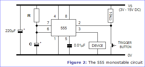
The circuit diagram of the 555 monostable circuit is given in figure 2. The value of R and C determine the length of time that it's output is in the high state. It can be calculated using the equation below...
![]()
...where T is the time period in seconds, and R and C are the component values in Ohms (Ω) and Farads (F).

Calculations
- Firstly, decide the time period T that you require. This can be very small (milliseconds) or large (minutes), but it must be expressed in seconds. {I choose T = 10 seconds}
- Next, guess a value for the capacitor C, expressed in Farads. For starters, try 100μF. {I choose C = 100μF}
- Put the values of T and C into the equation below and calculator resistor R...
![[Equation] [Equation]](http://www.eleinmec.com/equations/004_02.gif)
If the resistor value you calculated is smaller than 1kΩ or larger than 1MΩ, you should re-do the calculation with a different value for capacitor C until you get a resistor value within the acceptable range.
Varying the Time Period
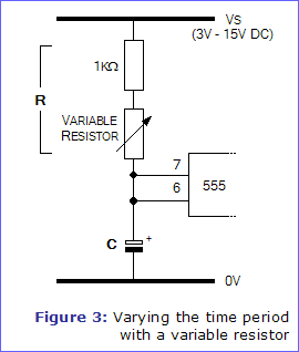
If you will need to adjust the time period of the monostable circuit in use, you can use a linear variable resistor for R, as shown in figure 3.
Because the resistance of a variable resistor goes down to around 0Ω at one end of its range, a 1kΩ resistor is placed in series with it so that the value of R will never fall below 1kΩ. As the shaft of the variable resistor is turned from its lowest setting to its highest, T will become longer.
If your chosen variable resistor has three connections, it is a potentiometer, and you should connect to the centre connection and either of the end connections.
| Further Information | Resistors - Includes information about variable resistors |

The Trigger Input
As you can see from figure 1, the 555's Trigger input must be taken low to trigger the monostable. This is achieved in figure 2 by placing a button in series with a resistor across the power supply. Normally, the 10kΩ resistor keeps the Trigger input high, at the voltage Vs, and the monostable is in its steady state. When the button is pushed, the Trigger input is directly connected to 0V and the time period T starts.
The Reset Input
If you want to make the monostable output go low before the time period has elapsed, simply take the 555's Reset input briefly low. This can be achieved with a push button in exactly the same way as with the Trigger input.
Astable Operation
 With the output high (+Vs) the capacitor C1 is charged by current flowing through R1 and R2. The threshold and trigger inputs monitor the capacitor voltage and when it reaches 2/3Vs (threshold voltage) the output becomes low and the discharge pin is connected to 0V.
The capacitor now discharges with current flowing through R2 into the discharge pin. When the voltage falls to 1/3Vs (trigger voltage) the output becomes high again and the discharge pin is disconnected, allowing the capacitor to start charging again.
This cycle repeats continuously unless the reset input is connected to 0V which forces the output low while reset is 0V.
An astable can be used to provide the clock signal for circuits such as counters.
A low frequency astable (<>
An audio frequency astable (20Hz to 20kHz) can be used to produce a sound from a loudspeaker or piezo transducer. The sound is suitable for buzzes and beeps. The natural (resonant) frequency of most piezo transducers is about 3kHz and this will make them produce a particularly loud sound.
Duty cycle
The duty cycle of an astable circuit is the proportion of the complete cycle for which the output is high (the mark time). It is usually given as a percentage.For a standard 555/556 astable circuit the mark time (Tm) must be greater than the space time (Ts), so the duty cycle must be at least 50%:
| Duty cycle = | Tm | = | R1 + R2 |
| Tm + Ts | R1 + 2R2 |
 |
555 Astable Multivibrator
 |
| 555 astable output, a square wave (Tm and Ts may be different) |
 |
| 555 astable circuit |
| T = 0.7 × (R1 + 2R2) × C1 and f = | 1.4 |
| (R1 + 2R2) × C1 |
T = time period in seconds (s)
f = frequency in hertz (Hz)
R1 = resistance in ohms (
R2 = resistance in ohms (
C1 = capacitance in farads (F)
The time period can be split into two parts: T = Tm + Ts
Mark time (output high): Tm = 0.7 × (R1 + R2) × C1
Space time (output low): Ts = 0.7 × R2 × C1
Choosing R1, R2 and C1
| 555 astable frequencies | |||
| C1 | R2 = 10k R1 = 1k | R2 = 100k R1 = 10k | R2 = 1M R1 = 100k |
| 0.001µF | 68kHz | 6.8kHz | 680Hz |
| 0.01µF | 6.8kHz | 680Hz | 68Hz |
| 0.1µF | 680Hz | 68Hz | 6.8Hz |
| 1µF | 68Hz | 6.8Hz | 0.68Hz |
| 10µF | 6.8Hz | 0.68Hz (41 per min.) | 0.068Hz (4 per min.) |
- Choose C1 to suit the frequency range you require (use the table as a guide).
- Choose R2 to give the frequency (f) you require. Assume that R1 is much smaller than R2 (so that Tm and Ts are almost equal), then you can use:
R2 = 0.7 f × C1 - Choose R1 to be about a tenth of R2 (1k
 min.) unless you want the mark time Tm to be significantly longer than the space time Ts.
 - If you wish to use a variable resistor it is best to make it R2.
- If R1 is variable it must have a fixed resistor of at least 1k
 in series
(this is not required for R2 if it is variable).
Tuesday, July 6, 2010
Decade Counter
Decade Counter
The counter operates as a normal counter until it reaches a count of 10102, or 1010. At that time, both inputs to the NAND gate are HIGH, and the output goes LOW. This LOW applied to the CLR input of the FFs causes them to reset to 0. Remember from the discussion of J-K FFs that CLR and PS or PR override any existing condition of the FF. Once the FFs are reset, the count may begin again. The following table shows the binary count and the inputs and outputs of the NAND gate for each count of the decade counter:
| BINARY COUNT | NAND GATE INPUTS | NAND GATE OUTPUT | |
| ******* | A | B | ******* |
| 0000 | 0 | 0 | 1 |
| 0001 | 0 | 0 | 1 |
| 0010 | 1 | 0 | 1 |
| 0011 | 1 | 0 | 1 |
| 0100 | 0 | 0 | 1 |
| 0101 | 0 | 0 | 1 |
| 0110 | 1 | 0 | 1 |
| 0111 | 1 | 0 | 1 |
| 1000 | 0 | 1 | 1 |
| 1001 | 0 | 1 | 1 |
Changing the inputs to the NAND gate can cause the maximum count to be changed. For instance, if FF4 and FF3 were wired to the NAND gate, the counter would count to 11002 (1210), and then reset.
7 Segment Counter Circuit


